
Analog-to-Digital Converter (ADC)
This experiment introduces analog-to-digital conversion using the TM4C123’s dual 12-bit ADC modules. You will configure sample sequencers for automatic multi-channel data acquisition, implement both polling and interrupt-driven sampling modes, and interface with analog sensors such as potentiometers and the internal temperature sensor. By the end of this lab, you will understand how to convert continuous analog signals to discrete digital values, configure trigger sources for periodic sampling, and implement sensor interfacing applications that bridge the analog and digital domains.
Objectives
- Understand analog-to-digital conversion principles including sampling, quantization, and resolution.
- Recognize the architecture of the TM4C123 ADC modules including dual 12-bit converters and shared input channels.
- Configure ADC sample sequencers (SS0-SS3) with different depths and trigger sources.
- Configure GPIO pins for analog input using AFSEL, AMSEL, and DEN registers.
- Implement software-triggered and hardware-triggered ADC conversions.
- Read and interpret ADC conversion results from FIFO registers.
- Convert digital ADC values to physical quantities such as voltage and temperature.
- Implement both polling and interrupt-driven ADC operation modes.
Background
Introduction to Analog-to-Digital Conversion
Analog-to-Digital Converters (ADCs) are essential components in embedded systems, enabling microcontrollers to interface with the analog world by converting continuous analog signals (such as voltage from sensors) into discrete digital values for processing. They are widely used in applications like temperature sensing, light intensity measurement, and audio signal processing.
ADC Resolution and Sampling
ADCs are characterized by their resolution, which indicates the number of discrete levels they can represent, typically expressed in bits. For instance, a 12-bit ADC can represent
where
TM4C123 ADC Architecture
The TM4C123GH6PM microcontroller features two identical 12-bit ADC modules (ADC0 and ADC1) that share 12 analog input channels. These modules provide high-precision conversion of continuous analog voltages to discrete digital numbers.
Key Features
The ADC modules offer the following capabilities:
- Resolution: 12-bit precision (0 to 4095 discrete levels)
- Shared Input Channels: 12 analog input channels (AIN0-AIN11) shared between both modules
- Internal Temperature Sensor: On-chip temperature measurement capability
- Maximum Sample Rate: 1 million samples per second (1 MSPS)
- Reference Voltage: VDDA = 3.3V (separate analog power supply)
- Input Voltage Range: 0V to 3.3V for single-ended inputs
- Sample Sequencers: Four programmable sequencers per module (SS0-SS3) with depths of 8, 4, 4, and 1 samples
- Hardware Averaging: Automatic averaging of up to 64 samples for noise reduction
- Digital Comparators: Eight digital comparators per module for threshold detection
- DMA Support: Dedicated μDMA channels for efficient data transfer with burst requests
- Isolated Power: Separate analog power and ground pins for improved signal integrity
ADC Input Channels
The TM4C123 provides 12 analog input channels (AIN0 to AIN11) that can be connected to various GPIO pins, shared between both ADC modules. The mapping is as follows:
| Channel | AIN0 | AIN1 | AIN2 | AIN3 | AIN4 | AIN5 | AIN6 | AIN7 | AIN8 | AIN9 | AIN10 | AIN11 |
|---|---|---|---|---|---|---|---|---|---|---|---|---|
| Pin | PE3 | PE2 | PE1 | PE0 | PD3 | PD2 | PD1 | PD0 | PE5 | PE4 | PB4 | PB5 |
ADC Input Channel Pin Mapping
Sample Sequencers
Each ADC module has four independent sample sequencers that manage sampling control and data capture autonomously. They differ only in the number of samples and FIFO depth.
| Sequencer | Number of Samples | FIFO Depth | Priority |
|---|---|---|---|
| SS0 | 8 | 8 entries | Highest |
| SS1 | 4 | 4 entries | High |
| SS2 | 4 | 4 entries | Low |
| SS3 | 1 | 1 entry | Lowest |
Sample Sequencer Capabilities and FIFO Depths
Trigger Sources
ADC conversions can be initiated by various trigger sources for flexibility:
- Processor (Software): Manual trigger via ADCPSSI register
- Analog Comparators: Trigger on comparator output events
- GPIO: External signal on GPIO pins
- General-Purpose Timers: Periodic sampling synchronized with timer events
- PWM Generators: Synchronize sampling with PWM signals for motor control
- Continuous: Free-running continuous sampling mode
Internal Temperature Sensor
The internal temperature sensor can be sampled by setting the TSn bit in the ADCSSCTLn register. Temperature (TEMP in °C) is calculated from the ADC reading (ADCCODE, 0 to 4095) as:
Note: This measures the microcontroller’s die temperature, not ambient, and is useful for thermal management but may require calibration.
ADC Registers
The TM4C123 ADC modules are configured via registers. Refer to the datasheet for details. Key registers include:
RCGCADC — ADC Run Mode Clock Gating Control
Enables/disables clock for ADC modules. Bits correspond to modules (1 = enable, 0 = disable).
RCGCADC Register — ADC Run Mode Clock Gating Control
| Bits | Field |
|---|---|
| 31–16 | reserved |
| 15–2 | reserved |
| 1 | ADC1 |
| 0 | ADC0 |
ADCACTSS — ADC Active Sample Sequencer
Enables/disables sample sequencers. Bits correspond to sequencers (1 = enable, 0 = disable). BUSY indicates ADC status (1 = busy, 0 = idle).
ADCACTSS Register — ADC Active Sample Sequencer
| Bits | Field |
|---|---|
| 31–17 | reserved |
| 16 | BUSY |
| 15–4 | reserved |
| 3 | SS3 |
| 2 | SS2 |
| 1 | SS1 |
| 0 | SS0 |
ADCSSMUXn — ADC Sample Sequence Input Multiplexer Select
Selects input channels for each sample in a sequencer. Each 4-bit field (MUX0-MUX7) specifies the channel (0-11 for AIN0-AIN11).
ADCSSMUXn Register — ADC Sample Sequence Input Multiplexer Select
| Bits | Field |
|---|---|
| 31–28 | MUX7 |
| 27–24 | MUX6 |
| 23–20 | MUX5 |
| 19–16 | MUX4 |
| 15–12 | MUX3 |
| 11–8 | MUX2 |
| 7–4 | MUX1 |
| 3–0 | MUX0 |
ADCSSCTLn — ADC Sample Sequence Control
Configures each sample in a sequence. The END bit must be set for the final sample. This 32-bit register handles up to eight samples.
ADCSSCTLn Register — ADC Sample Sequence Control
| Bits | Field |
|---|---|
| 31 | TS7 |
| 30 | IE7 |
| 29 | END7 |
| 28 | D7 |
| 27 | TS6 |
| 26 | IE6 |
| 25 | END6 |
| 24 | D6 |
| 23 | TS5 |
| 22 | IE5 |
| 21 | END5 |
| 20 | D5 |
| 19 | TS4 |
| 18 | IE4 |
| 17 | END4 |
| 16 | D4 |
| 15 | TS3 |
| 14 | IE3 |
| 13 | END3 |
| 12 | D3 |
| 11 | TS2 |
| 10 | IE2 |
| 9 | END2 |
| 8 | D2 |
| 7 | TS1 |
| 6 | IE1 |
| 5 | END1 |
| 4 | D1 |
| 3 | TS0 |
| 2 | IE0 |
| 1 | END0 |
| 0 | D0 |
Where:
- TSx: Temperature sensor select (1 = sample temperature sensor)
- IEx: Interrupt enable (1 = enable interrupt on sample completion)
- ENDx: End of sequence (1 = last sample in sequence)
- Dx: Differential select (1 = differential input, 0 = single-ended)
- x: Sample index (0-7)
ADCEMUX — ADC Event Multiplexer Select
Selects trigger source for each sample sequencer. Each 4-bit field (EM0-EM3) specifies the trigger source.
ADCEMUX Register — ADC Event Multiplexer Select
| Bits | Field |
|---|---|
| 31–16 | reserved |
| 15–12 | EM3 |
| 11–8 | EM2 |
| 7–4 | EM1 |
| 3–0 | EM0 |
The EMx field specifies the trigger source for sample sequencer x:
| Value | Trigger Source |
|---|---|
| 0x0 | Processor (software trigger via ADCPSSI register) |
| 0x1 | Analog Comparator 0 |
| 0x2 | Analog Comparator 1 |
| 0x3 | Reserved |
| 0x4 | External GPIO (connected to GPIO interrupt) |
| 0x5 | Timer (requires TnOTE bit set in GPTMCTL register) |
| 0x6 | PWM Generator 0 |
| 0x7 | PWM Generator 1 |
| 0x8 | PWM Generator 2 |
| 0x9 | PWM Generator 3 |
| 0xA–0xE | Reserved |
| 0xF | Continuous (always sampling) |
ADC Event Multiplexer Trigger Sources
Timer-triggered sampling (EM = 0x5): this hooks a GPTM directly to the ADC without any CPU involvement at sample time. Configure the timer (as in Experiment 7) in periodic mode, then set its TnOTE bit (bit 5 of TIMERx->CTL for Timer A, bit 13 for Timer B — the same CTL register from Experiment 7’s GPTM section) so that each timeout pulses the ADC trigger instead of (or in addition to) generating a CPU interrupt. Set the corresponding sequencer’s ADCEMUX field to 0x5, and the ADC samples automatically every time the timer expires — this is what Task 1 asks you to wire up.
ADCPSSI — ADC Processor Sample Sequence Initiate
Initiates sampling for the specified sample sequencer when triggered by the processor.
ADCPSSI Register — ADC Processor Sample Sequence Initiate
| Bits | Field |
|---|---|
| 31 | GSYNC |
| 30–28 | reserved |
| 27 | SYNCWAIT |
| 26–16 | reserved |
| 15–4 | reserved |
| 3 | SS3 |
| 2 | SS2 |
| 1 | SS1 |
| 0 | SS0 |
Where:
- SSx: Sample Sequencer x Initiate (write 1 to trigger conversion, self-clearing)
- SYNCWAIT: Synchronize Wait (1 = wait for synchronization signal before initiating)
- GSYNC: Global Synchronize (1 = generate synchronization signal for multiple ADC modules)
Note: The SSx bits are write-only and automatically clear after initiating the conversion. For synchronized sampling across modules, set GSYNC in one module to trigger all modules with SYNCWAIT enabled.
ADCSSFIFOn — ADC Sample Sequence FIFO
Holds the conversion results for the specified sample sequencer. Each read retrieves the next sample from the FIFO.
ADCSSFIFOn Register — ADC Sample Sequence FIFO
| Bits | Field |
|---|---|
| 31–16 | reserved |
| 15–12 | reserved |
| 11–0 | DATA |
Where:
- DATA: 12-bit conversion result (0 to 4095)
- reserved: Unused bits
You can read from the ADCSSFIFOn register to retrieve conversion results. Each read operation removes the oldest sample from the FIFO. Ensure that the FIFO is not empty before reading to avoid invalid data. You can check the FIFO status using the ADCSSSTAT register (refer to the datasheet for details).
ADCRIS — ADC Raw Interrupt Status
Holds the raw interrupt status for each sample sequencer.
ADCRIS Register — ADC Raw Interrupt Status
| Bits | Field |
|---|---|
| 31–17 | reserved |
| 16 | INRDC |
| 15–4 | reserved |
| 3 | SS3 |
| 2 | SS2 |
| 1 | SS1 |
| 0 | SS0 |
Where:
- SSx: Sample Sequencer x Interrupt Status (1 = interrupt pending, 0 = no interrupt)
- INRDC: Digital Comparator Raw Interrupt Status
- reserved: Unused bits
ADCIM — ADC Interrupt Mask
Masks/unmasks interrupts for each sample sequencer.
ADCIM Register — ADC Interrupt Mask
| Bits | Field |
|---|---|
| 31–20 | reserved |
| 19 | DCONSS3 |
| 18 | DCONSS2 |
| 17 | DCONSS1 |
| 16 | DCONSS0 |
| 15–4 | reserved |
| 3 | MASK3 |
| 2 | MASK2 |
| 1 | MASK1 |
| 0 | MASK0 |
Where:
- MASKx: Sample Sequencer x Interrupt Mask (1 = unmask interrupt, 0 = mask interrupt)
- DCONSSx: Digital Comparator Interrupt Mask for Sample Sequencer x (1 = unmask comparator interrupt, 0 = mask comparator interrupt)
- x: Sample sequencer index (0-3)
- reserved: Unused bits
ADCISC — ADC Interrupt Status and Clear
Holds and clears the interrupt status for each sample sequencer.
ADCISC Register — ADC Interrupt Status and Clear
| Bits | Field |
|---|---|
| 31–20 | reserved |
| 19 | DCINSS3 |
| 18 | DCINSS2 |
| 17 | DCINSS1 |
| 16 | DCINSS0 |
| 15–4 | reserved |
| 3 | IN3 |
| 2 | IN2 |
| 1 | IN1 |
| 0 | IN0 |
Where:
- SSx: Sample Sequencer x Interrupt Clear (write 1 to clear interrupt)
- DCINSSx: Digital Comparator Interrupt Clear for Sample Sequencer x (write 1 to clear comparator interrupt)
- reserved: Unused bits
GPIO Registers
To configure GPIO pins for ADC input, you will need to set the appropriate GPIO registers. Below are the key registers involved in configuring GPIO pins for analog input:
GPIODEN — GPIO Digital Enable
Enables/disables digital functionality for GPIO pins. To use a pin as an analog input, its corresponding bit in this register must be cleared (0 = disable digital function).
GPIODEN Register (Port x) — Digital Enable
| Bits | Field |
|---|---|
| 31–16 | reserved |
| 15–8 | reserved |
| 7 | Px7 |
| 6 | Px6 |
| 5 | Px5 |
| 4 | Px4 |
| 3 | Px3 |
| 2 | Px2 |
| 1 | Px1 |
| 0 | Px0 |
Where:
- Pxn: Digital Enable for Pin n of Port x (1 = enable digital function, 0 = disable digital function)
- reserved: Unused bits
- x: Port letter (A-F)
- n: Pin number (0-7)
Note: To configure a pin for analog input, clear its corresponding bit in the GPIODEN register.
GPIOAFSEL — GPIO Alternate Function Select
Selects alternate functions for GPIO pins. To use a pin for ADC input, its corresponding bit in this register must be set (1 = alternate function enabled).
GPIOAFSEL Register (Port x) — Alternate Function Select
| Bits | Field |
|---|---|
| 31–16 | reserved |
| 15–8 | reserved |
| 7 | Px7 |
| 6 | Px6 |
| 5 | Px5 |
| 4 | Px4 |
| 3 | Px3 |
| 2 | Px2 |
| 1 | Px1 |
| 0 | Px0 |
Where:
- Pxn: Alternate Function Select for Pin n of Port x (1 = enable alternate function, 0 = GPIO function)
- reserved: Unused bits
- x: Port letter (A-F)
- n: Pin number (0-7)
Note: To configure a pin for ADC input, set its corresponding bit in the GPIOAFSEL register.
GPIOAMSEL — GPIO Analog Mode Select
Enables/disables analog functionality for GPIO pins. To use a pin as an analog input, its corresponding bit in this register must be set (1 = enable analog function).
GPIOAMSEL Register (Port x) — Analog Mode Select
| Bits | Field |
|---|---|
| 31–16 | reserved |
| 15–8 | reserved |
| 7 | Px7 |
| 6 | Px6 |
| 5 | Px5 |
| 4 | Px4 |
| 3 | Px3 |
| 2 | Px2 |
| 1 | Px1 |
| 0 | Px0 |
Where:
- Pxn: Analog Mode Select for Pin n of Port x (1 = enable analog function, 0 = disable analog function)
- reserved: Unused bits
- x: Port letter (A-F)
- n: Pin number (0-7)
Note: To configure a pin for ADC input, set its corresponding bit in the GPIOAMSEL register.
Configuration Steps
Configuring a GPIO pin for ADC input on the TM4C123 microcontroller involves three stages:
GPIO Pin Configuration
To prepare a GPIO pin for analog input:
- Enable the clock for the corresponding GPIO port by setting the appropriate bit in the
RCGCGPIOregister. - Enable the pin’s alternate function using the
GPIOAFSELregister. - Disable its digital function by clearing the pin’s bit in the
GPIODENregister. - Enable the analog function by setting the pin’s bit in the
GPIOAMSELregister. - Set the pin direction as input by clearing its bit in the
GPIODIRregister. (OnceAMSELis set,GPIODIRno longer affects the pin’s electrical behavior — the analog circuitry takes over regardless of this bit — but clearing it is still good practice so the pin’s configuration is unambiguous if analog mode is ever disabled later.)
ADC Sampling Sequencer Setup
After the pin is configured, the ADC module and sampling sequencer must be set up:
- Enable the ADC clock by setting the correct bit in the
RCGCADCregister. - Disable the chosen sample sequencer by clearing its bit in the
ADCACTSSregister. - Select the input channel(s) by configuring the
ADCSSMUXnregister. - Set the control options for each sample (e.g., END, IE) in the
ADCSSCTLnregister, ensuring the END bit is set for the final sample. - Choose the trigger source by configuring the
ADCEMUXregister. - Re-enable the sequencer by setting its bit in
ADCACTSS. - If processor-triggered sampling is used, start a conversion using the
ADCPSSIregister.
Interrupt Configuration
If interrupts are required:
- Enable interrupts for the selected sequencer by setting its bit in the
ADCIMregister. - Enable the corresponding interrupt in the NVIC by setting the appropriate bit in the
NVIC_ISERregister. - In the ISR, read the conversion result from the
ADCSSFIFOregister. - Clear the interrupt flag by writing to the appropriate bit in the
ADCISCregister.
Examples
Setting up the project
This experiment runs on the TM4C123 LaunchPad. If you haven't made a project yet, follow the Tiva LaunchPad Project guide first, and make sure its blinking-LED test works.
Target device: TM4C123GH6PM
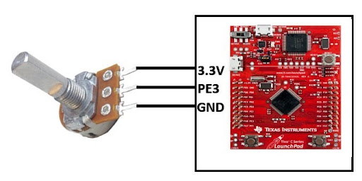
This section demonstrates how to configure and use the ADC module on the TM4C123 microcontroller using both polling and interrupt-driven sampling methods. A potentiometer is used as a controllable analog input source by wiring its terminals to 3.3 V and ground, with the adjustable rotor connected to an ADC input such as AIN0 (PE3). Rotating the potentiometer varies the rotor voltage between 0 V and 3.3 V, allowing you to generate different analog levels and observe the corresponding ADC conversion results.
Example 1: Single ADC Channel Reading (Polling Method)
In this example, you will configure the ADC to read a single analog input channel (AIN0) using sample sequencer 3 (SS3) and turn on an LED if the voltage exceeds a certain threshold.
#include "TM4C123.h"
#define GREEN_LED 1 << 3
volatile unsigned int adc_value;
int main(void)
{
    SYSCTL->RCGCGPIO |= (1 << 4); // Enable Clock to GPIOE or PE3/AN0
    SYSCTL->RCGCADC |= (1 << 0);  // AD0 clock enable

    GPIOE->AFSEL |= (1 << 3);  // enable alternate function
    GPIOE->DEN &= ~(1 << 3);   // disable digital function
    GPIOE->AMSEL |= (1 << 3);  // enable analog function
    GPIOE->DIR &= ~(1 << 3);   // clear direction bit (don't-care once AMSEL is set, but good practice)

    ADC0->ACTSS &= ~(1 << 3);            // disable SS3 during configuration
    ADC0->EMUX &= ~0xF000;                // Software Trigger
    ADC0->SSMUX3 = 0;                    // get input from channel 0
    ADC0->SSCTL3 |= (1 << 1) | (1 << 2); // take one sample at a time, set flag at 1st sample
    ADC0->ACTSS |= (1 << 3);             // enable ADC0 sequencer 3

    SYSCTL->RCGCGPIO |= 0x20; // turn on bus clock for GPIOF
    GPIOF->DIR |= GREEN_LED;       // set GREEN pin as a digital output pin
    GPIOF->DEN |= GREEN_LED;       // Enable PF3 pin as a digital pin

    while (1)
    {
        ADC0->PSSI |= (1 << 3);            // initiate SS3 conversion
        while ((ADC0->RIS & (1<<3)) == 0);      // Wait untill sample conversion completed
        adc_value = ADC0->SSFIFO3;         // read adc coversion result from SS3 FIFO
        ADC0->ISC = (1<<3);                     // clear coversion clear flag bit

        if (adc_value >= 2048)
            GPIOF->DATA |= GREEN_LED; // turn on green LED
        else if (adc_value < 2048)
            GPIOF->DATA &= ~GREEN_LED; // turn off green LED
    }
}
Example 2: Reading Internal Temperature Sensor
In this example, you will configure the ADC to read the internal temperature sensor using sample sequencer 3 (SS3) and display the temperature value on the debugger using the Watch window.
- Start a debug session: After building the program successfully, start a debug session in Keil uVision IDE (Ctrl + F5).
- Add variables to the Watch window: select the variable name in the code, right-click, and choose "Add to Watch", or enter the variable name in the Watch window manually.
- Run the program: Use the "Run" button (F5) to execute the program. The Watch window will update with the current values of the monitored variables.
#include "TM4C123.h"

volatile unsigned int adc_value;
volatile float temp;

void ADC0SS3_Handler(void)
{
    adc_value = ADC0->SSFIFO3 & 0xFFF; // Read 12-bit ADC value from FIFO
    temp = 147.5 - (75 * 3.3f * adc_value)/ 4096; // Convert to temperature in Celsius
    ADC0->ISC = (1<<3); // Clear SS3 interrupt flag
}

int main(void)
{
    SYSCTL->RCGCGPIO |= (1 << 4); // Enable clock to Port E
    SYSCTL->RCGCADC |= (1 << 0);  // Enable clock to ADC0

    GPIOE->AFSEL |= (1 << 3);  // Enable alternate function on PE3
    GPIOE->DEN &= ~(1 << 3);   // Disable digital I/O on PE3
    GPIOE->AMSEL |= (1 << 3);  // Enable analog input on PE3
    GPIOE->DIR &= ~(1 << 3);   // Clear direction bit (don't-care once AMSEL is set, but good practice)

    ADC0->ACTSS &= ~(1 << 3);            	// Disable SS3 during configuration
    ADC0->EMUX |= 0xF000;               	// Set SS3 to continuous sampling mode
    ADC0->SSMUX3 = 0;                    	// Configure SS3 to sample AIN0 (PE3)
    ADC0->SSCTL3 |= (1 << 1) | (1 << 2) | (1 << 3); 	// Set end of sequence, enable interrupt, enable temperature sensor

    ADC0->IM |= (1 << 3);        // Enable SS3 interrupt mask
    NVIC_EnableIRQ(ADC0SS3_IRQn); // Enable ADC0 SS3 interrupt in NVIC

    ADC0->ACTSS |= (1 << 3);  // Enable SS3

    while (1) {} // Wait for interrupts
}
Code Explanation
GPIO/ADC Setup: Both examples follow the same pattern: enable the RCGCGPIO and RCGCADC clocks, then put PE3 into analog mode (AFSEL, DEN, AMSEL, DIR).
Sequencer Configuration: ADC0->ACTSS disables SS3 while it's being configured, ADC0->EMUX selects the trigger source (software in Example 1, continuous in Example 2), ADC0->SSMUX3 = 0 selects input channel AIN0, and ADC0->SSCTL3 marks the sample as the end of the sequence (and, in Example 2, additionally selects the internal temperature sensor and enables its per-sample interrupt).
Example 1 — Polling: The main loop writes ADCPSSI to start a conversion, spins on ADCRIS until the raw-status bit for SS3 is set, reads the result from ADCSSFIFO3, and clears the flag via ADCISC, all under software control with no interrupt involved.
Example 2 — Interrupt-Driven: ADC0->IM unmasks the SS3 interrupt and NVIC_EnableIRQ(ADC0SS3_IRQn) enables it in the NVIC. Because EMUX is set to continuous mode, the ADC keeps sampling on its own and ADC0SS3_Handler() fires after every conversion: it reads SSFIFO3, converts the result to a temperature, and clears the interrupt flag via ADCISC. The main loop does nothing but wait.
Lab work
Lab work 1: Timer-Based Temperature Measurement
Modify Example 2 so that the ADC sampling is triggered by a timer every second, instead of using continuous sampling mode. Connect an analog temperature sensor (e.g., TMP36) to an ADC input channel (such as AIN0 on PE3). Configure the ADC to read the sensor voltage on each timer trigger and calculate the corresponding temperature. Monitor the temperature values in real time by adding the variable temp to the Watch window in the debugger.
Lab work 2: Comparing Two ADC Channels Using Dual Modules
Extend Example 2 to read two different analog inputs using separate ADC modules: use the ADC0 module to sample AIN0 (PE3) and the ADC1 module to sample AIN1 (PE2), both with sample sequencer 3 (SS3). Configure both ADC modules to use interrupts so that each conversion triggers its respective ISR. In the interrupt handlers, compare the two ADC values and use the result to control LEDs on GPIOF: for example, turn on the green LED if ADC0's value is higher, or turn on the red LED if ADC1's value is higher. This demonstrates simultaneous sampling using both ADC modules. Display both ADC values in the debugger Watch window to observe the comparison in real time.